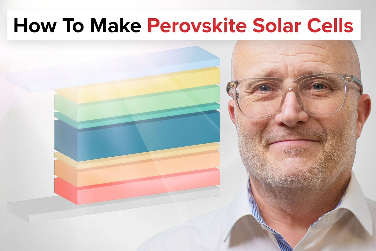
How to Prepare the First Charge Selective Layer in Perovskite Solar Cells
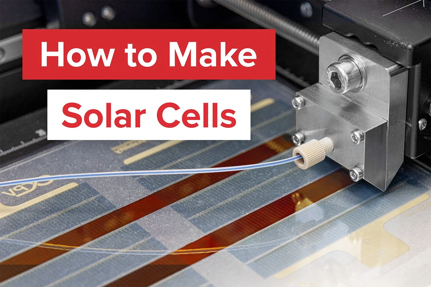
As part of our video series on manufacturing perovskite solar cells and modules using roll-to-roll processing, we provide a detailed walkthrough of each layer and process step required to successfully reproduce the technology in your own laboratory.
Using compact laboratory equipment capable of producing many square meters per run, this approach is designed to fit within a standard laboratory environment while maintaining scalability and precision.
In this article, we focus on the preparation of the first charge selective layer, an essential step in defining device architecture and performance. This layer can function as either a hole selective layer or an electron selective layer, and several well-established methods are available to achieve this.
In this article, we focus on the preparation of the first charge selective layer.
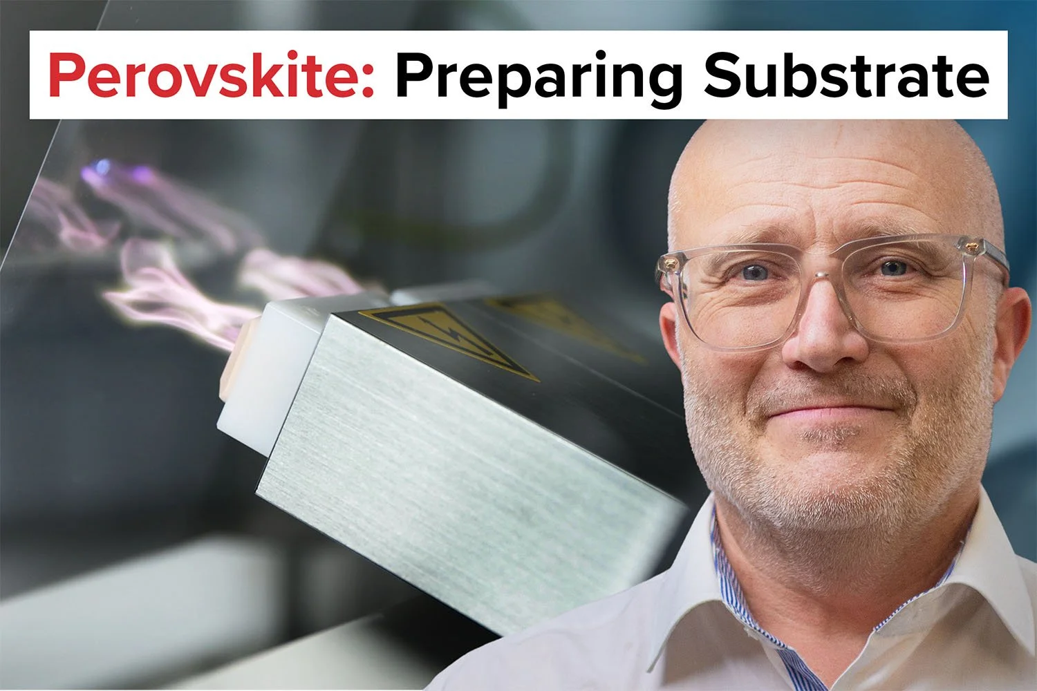
Preparing the Substrate and Defining the Stack
Before applying the first charge selective layer, the substrate carrier must first be selected, cleaned, and, if necessary, patterned. Patterning can be achieved by printing the desired electrode structure, laser scribing the required design, or selectively etching away ITO in areas where conductivity is not needed.
Once the substrate is prepared, the next step is selecting the perovskite solar cell stack.
One of the first and most important decisions is determining how charge carriers will be transported through the stack.
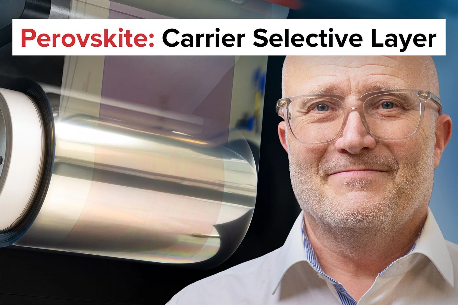
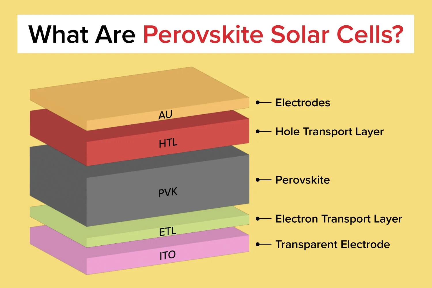
This is accomplished by printing or coating a charge selective layer on top of the ITO. The purpose of this layer is to allow one type of charge carrier, either holes or electrons, to pass through to the ITO while blocking the other.
This initial choice strongly influences how all subsequent layers are selected and processed. Depending on whether the electron selective layer or the hole selective layer is applied first, the stack is referred to as either an N-I-P or a P-I-N structure.
P-I-N and N-I-P Stacks.
Electron Selective Layers for N-I-P Stacks
In the N-I-P stack configuration, one of the most commonly used electron transporting layers is tin oxide (SnO2), which performs particularly well with the perovskite active layer.
SnO2 can be applied by slot-die coating either as a fully covering layer or in stripes. The material can be processed from either a water-based solution or an organic alcohol such as ethanol or isopropanol.
A common example is the preparation of highly uniform SnO2 layers using a water-based dispersion of tin oxide nanoparticles. After drying, the resulting layer is approximately 40 nm thick and ready for use.
Another widely used option is zinc oxide (ZnO), which can also be slot-die coated using a nanoparticle dispersion in acetone or isopropanol. The process follows the same principles, producing a final dry thickness of approximately 100 nm.
Both SnO2 and ZnO function as effective electron transporting layers and provide strong starting points for N-I-P device structures.
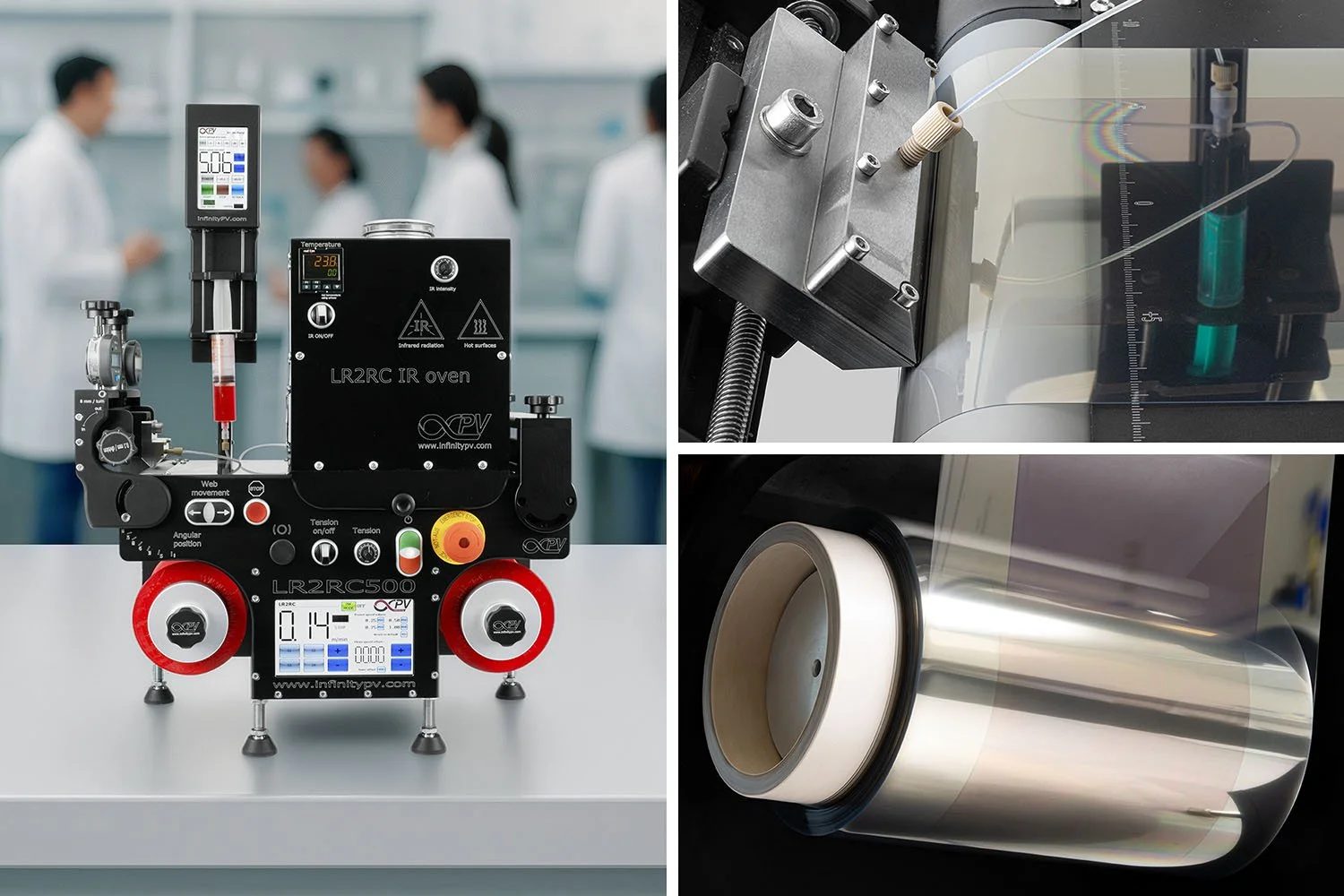
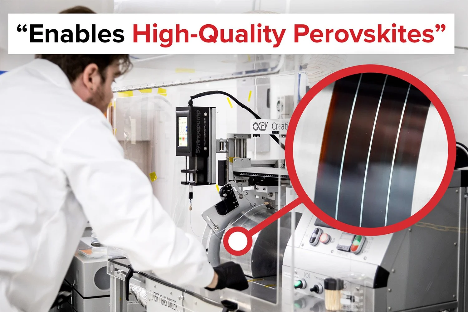
In this series, we use the Laboratory Roll-to-Roll Coater to slot-die coat the various layers.
Hole Selective Layers for P-I-N Stacks
For P-I-N stack configurations, one of the best-known metal oxide layers is nickel oxide (NiO), which serves as a hole transporting layer.
NiO can be slot-die coated from a nanoparticle dispersion in ethanol. Although the NiO suspension itself is coloured, the final coated layer is extremely thin, resulting in a semitransparent film on top of the ITO.
Another attractive approach for P-I-N structures is the use of a self-assembled monolayer (SAM) on top of the ITO, which also functions as a hole selective layer.
Because a SAM forms an extremely thin layer, it offers significant advantages in terms of material efficiency and interface quality. Typically, the SAM material consists of a simple molecule such as an electron-rich aromatic compound like carbazole. This molecule can be anchored to the ITO surface using a functional group with strong affinity for ITO, such as a phosphonic acid group.
This creates an effective and highly controlled interface for hole transport.
Self-assembled monolayer (SAM) on top of the ITO.
Ready for the Active Layer
Once the first charge selective layer has been successfully applied to the substrate and electrode, the stack is ready for the next stage: deposition of the active perovskite layer.
This step is critical for device performance and will be covered in the next part of the series, where we demonstrate how to apply the active perovskite layer using roll-to-roll compatible processing methods.
Explore the Entire How To Make Perovskite Series
Learn how to make perovskite solar cells. Each single layer. We’ll show you how.
Related Articles


Related Products

Laboratory Roll-to-Roll Coater
A compact and modular high precision roll-to-roll slot-die coater that transforms the way thin functional films are printed and coated.

Slot-die Coater
A state-of-the-art, compact sheet coater for precise, consistent slot-die coatings, featuring a vacuum chuck, integrated drying, and optimized ink delivery.

LR2RC500 Bundle
Probably the world’s most compact R2R slot-die coater. A compact, fully integrated R2R coater that fits on a workbench, in a fume hood or a glovebox.

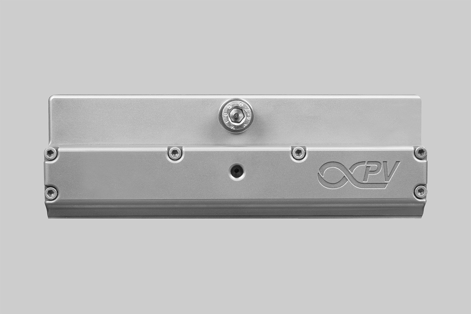
Slot-die Heads
Slot-die heads for high-quality coatings. Available in stainless steel, titanium, or PEEK, with widths from 40 mm to 305 mm, ensuring precise thin-film production.


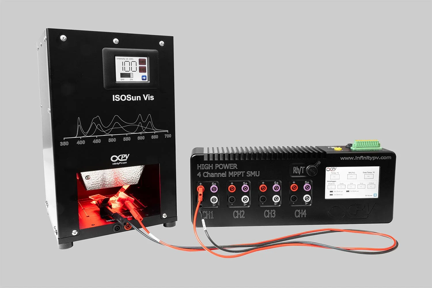

Get started with solar cell research with a complete, ready-to-use system. This bundle combines a compact Solar Simulator and an 8 Channel Source Measure Unit to make PV characterization easy and accessible.